Original Link: https://www.anandtech.com/show/7591/answered-by-the-experts-arms-cortex-a53-lead-architect-peter-greenhalgh
Answered by the Experts: ARM's Cortex A53 Lead Architect, Peter Greenhalgh
by Anand Lal Shimpi on December 17, 2013 11:56 PM EST- Posted in
- Ask the Experts
Last week we held an awesome Ask the Experts Q&A with ARM's Peter Greenhalgh, lead architect for the Cortex A53. Peter did a great job answering questions in the comments, but for those of you who missed them we're compiling all of the Q&A here for you to go through.
On Friday, December 20th at 12:00PM ET, Peter will be joining me for a live Google Hangouts chat. We'll be posting more details on that later this week. For now, enjoy the responses!
Question from shodanshok
Hi, it would be interesting to know two thing:
- the cache memories (L1/L2) are write-back or write-through? Inclusive or exclusive?
- multiprocessor capabilities are limited to 4 cores or they can scale to 8+ cores without additional glue logic?
Thanks.
Answer
Hi Shodanshok,
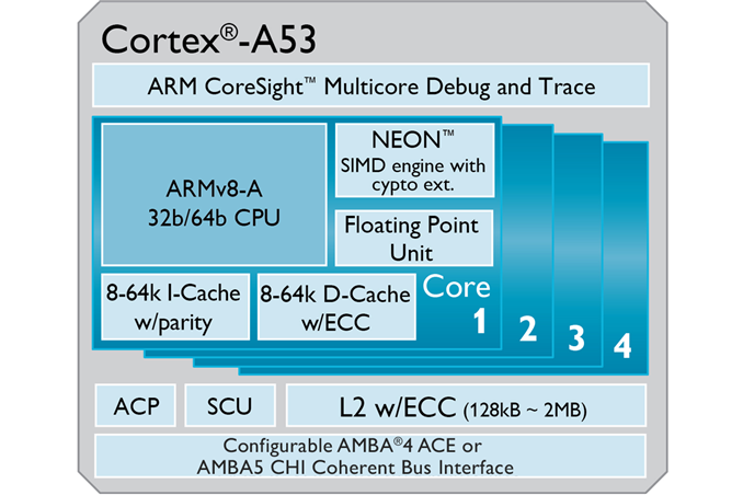
All cacheable attributes are supported, but Cortex-A53 is optimised around write-back, write-allocate. The L2 cache is inclusive on the instruction side and exclusive on the data side.
A Cortex-A53 cluster only supports up to 4-cores. If more than 4-cores are required in a platform then multiple clusters can be implemented and coherently connected using an interconnect such as CCI-400. The reason for not scaling to 8-cores per cluster is that the L2 micro-architecture would need to either compromise energy-efficiency in the 1-4 core range to achieve performance in the 4-8 core range, or compromise performance in the 4-8 core range to maximise energy-efficiency in the 1-4 core range. This isn’t a hard and fast rule for all clusters, but is the case for a cluster at the Cortex-A53 power/performance point. For the majority of mobile use cases it is best to focus on energy efficiency and enable more than 4-cores through multi-cluster solutions.
Question from lukarak
We have seen MediaTek introducing an 8xA7 SOC, instead of going to the big.LITTLE configuration of some sorts. Do you expect the same thing to happen with the A53 and A57 generation for low budget SOCs or will this generation's combo be a little easier and cheaper to implement?
Answer
Hi Lukarak,
We expect to see a range of platform configurations using Cortex-A53. A 4+4 Cortex-A53 platform configuration is fully supported and a logical progression from a 4+4 Cortex-A7 platform. A Cortex-A57 in the volume smartphone markets is less likely, but that’s a decision in the hands of the ARM partners. It will be interesting to see the range of Cortex-A53 platforms and configurations announced by partners over the coming months.
Question from ehsan.nitol
Hi there, I have some questions.
We have already seen how well Qualcomm's Cortex A7 can perform thanks to Moto G. How much will it improve with the new Cortex A53? What will be the core and performance wise difference? How will you compare it against Cortex A9, A12 and A15 in terms of performance, battery consumption and all.
With the Exynos Octa core processor Battery Test we haven't seen much battery improvements compared to Qualcomm's Snapdragon 600 and 800 Processor. How will it perform this time?
What is ARM planning do with its Mali GPU? What will be next after Cortex A53 and A57?
Answer
Hi Ehsan,
Cortex-A53 has the same pipeline length as Cortex-A7 so I would expect to see similar frequencies when implemented on the same process geometry. Within the same pipeline length the design team focussed on increasing dual-issue, in-order performance as far as we possibly could. This involved symmetric dual-issue of most of the instruction set, more forwarding paths in the datapaths, reduced issue latency, larger & more associative TLB, vastly increased conditional and indirect branch prediction resources and expanded instruction and data prefetching. The result of all these changes is an increase in SPECInt-2000 performance from 0.35-SPEC/Mhz on Cortex-A7 to 0.50-SPEC/Mhz on Cortex-A53. This should provide a noticeable performance uplift on the next generation of smartphones using Cortex-A53.
Question from Techguy99X
Why are the current A7 quad core phones performing similar to the A9 quad (exynos 4412 , tegra 3), although A9 is more advanced and OoO? What is the main difference between A5 and A7, becuase the A7 is just a bit faster than the A5?
Answer
Hi Techguy99X,
Overall platform performance is dependent on many factors including processor, interconnect, memory controller, GPU, video and more. While the Cortex-A9 is a higher performance processor both in IPC and frequency, ARM partners are continuously improving their platforms and porting them to new process geometries. This allows a new generation Cortex-A7 based platform to improve on an older generation Cortex-A9 based platform.
Compared to Cortex-A5, Cortex-A7 increased load-store bandwidth, allowed more common data-processing operations to dual-issue and made some small improvements in the branch-predictors.
Question from barleyguy
When designing a processor and deciding on which performance attributes to emphasize, do you target current workloads for short term market concerns, or do you target possible future workloads for the market a year or two from now? Or is performance tuning more workload agnostic, and do you say "I want this to be fast for everything"?
For example, since ARM processors are very popular in the Android market, do you tune for content comsumption and gaming? Or since Android may be trending towards more of a primary computing device in the future, is it important to tune for desktop applications?
And finally, what are the considerations of performance tuning for thermally constrained devices?
Answer
Hi Barleyguy,
A good question. A general purpose processor has to be good on all workloads. After all, we expect to see Cortex-A53 in everything from mobile phones to cars, set-top-box to micro-servers and routers. However we do track the direction software is evolving – for example the increased use of Javascript which puts pressure on structures such as indirect predictors. Therefore we design structures within the processor to cope with future code as well as existing expected workloads.
Question from psychobriggsy
Do you have any plans to support various forms of turbo functionality within your next generation ARM cores? An a potential example, in a 28nm quad-core A53 setup at 1.2GHz, you could support dual-core at >1.4GHz and single core at >1.6GHz within the same power consumption (core design allowing, of course), yet single threaded performance could improve significantly.
ARM cores have been historically low power, however that doesn't mean there aren't more power savings to be made. Examples include deeper sleep states, power gated cores, and so on - features that Intel and AMD have had to include in order to reduce their TDPs whereas ARM cores haven't need them (yet). What are the future power saving methods that ARM is considering for its future cores (that you can give away)?
Answer
Hi Psychobriggsy,
A Turbo mode is typically a form of voltage overdrive for brief periods of time to maximise performance, which ARM partners have been implementing on mobile platforms for many years. Whether this is applied to 1,2 or more cores is a decision of the Operating System and the platform power management software. If there is only one dominant thread you can bet that mobile platforms will be using Turbo mode. Due to the power-efficiency of Cortex-A53 on a 28nm platform, all 4 cores can comfortably be executing at 1.4GHz in less than 750mW which is easily sustainable in a current smartphone platform even while the GPU is in operation.
In terms of further power saving techniques, power gating unused cores is a technique that has been used since the first Cortex-A9 platforms appeared on the market several years ago. The technique is so fundamental that I think many in the mobile industry use it automatically and forget that it’s a highly beneficial power saving technique. But you are correct that there is more milage to come from deeper sleep states which is why both Cortex-A53 and Cortex-A57 support state retention techniques in caches and the NEON unit to further improve leakage power.
Question from Xebec
Peter, thanks for offering your time to Anandtech!
I was curious if you could talk a bit about how easy/difficult A53-derived SoCs might be to integrate into solutions that are already using A7/A9 type chips? i.e. Devices like Beagleboards, Raspberry Pis, ODROIDs, etc. Is there anything that makes the A53 particularly difficult or easy to suit to these types of devices?
Also, for Micro and "regular" servers, do you see A57/A53 big.LITTLE being the norm, or do you anticipate a variety of A53-only and A57-only designs? Any predictions on market split between the A5x series here?
Respectfully,
John
Answer
Hi Xebec,
Cortex-A53 has been designed to be able to easily replace Cortex-A7. For example, Cortex-A7 supports the same bus-interface standards (and widths) as Cortex-A7 which allows a partner who has already built a Cortex-A7 platform to rapidly convert to Cortex-A53.
With servers I think we will see a mix of solutions. The most popular approach will be to use Cortex-A57 due to the performance that micro-architecture is capable of providing, but I still expect some Cortex-A53 servers and big.LITTLE too!
Question from Doormat
ARM CPU vendors (Qualcomm, Nvidia, etc) seem to be choosing slower quad core over faster dual core, and I'm suspecting its all a marketing game (e.g. more cores is better, see Motorola's X8 announcement of an "8 core" phone). Do those non-technical decisions impact the decisions of the engineers in developing the ARM architecture?
Answer
Hi Doormat,
You are quite correct that there are a variety of frequencies and core-counts being offered by ARM partners. However, for ARM design micro-architectures these do not have an effect on micro-architectures as we must be able to support a variety of target frequencies and core-counts across many different process geometries.
Question from Factory Factory
How does designing a CPU "by hand" differ from using an automated layout tool? What sort of trade-offs does/would using automated tools cause for ARM's cores?
Second question: With many chips from many manufacturers now implementing technologies like fine-grained power gating, extremely fine control of power and clock states, and efficient out-of-order execution pipelines, where does ARM go from here to keep its leadership in low-power compute IP?
Answer
Hi Factory,
Hand layout versus automated layout is an interesting trade-off. From one perspective, full hand-layout for all circuits in a processor is rarely used now. Aside from cache RAMs which are always custom, hand-layout is reserved for datapath and queues which are regular structures that allow a human to spot the regularity and ‘beat’ an automated approach. However, control logic is not amenable to hand-layout as it’s very difficult to beat automated tools which means that the control logic can end up setting the frequency of the processor without significant effort.
In general the benefit from hand-layout has been reducing in recent years. Partly this is due to the complexity of the design rules for advanced process generations reducing the scope for more specific circuit tuning techniques to be used. But another factor is the development of advanced standard cell libraries that have a large variety of cells and drive strengths which lessens the need for special circuit techniques. When we’re developing our processors we’re fortunate to have access to a large team in ARM designing standard cell libraries and RAMs who can advise us about upcoming nodes (for example 16nm and 10nm). In turn the processor teams can suggest & trial new advanced cells for the libraries which we call POPs (Processor Optimization Packages) that improve frequency, power and area.
A final trade-off to consider is process portability. After an ARM processor is licensed we see it on many different process geometries which is only possible because the designs are fully synthesizable. For example, there are Cortex-A7 implementations on all the major foundries from 65nm to 16nm. In combination with the advanced standard cell libraries for these processes there is little need to go to a hand-layout approach and we instead enable our partners to get to market more rapidly on the process geometry and foundry of their choosing.
Question from mrdude
A few questions:
When can we expect an end to software based dvfs scaling? It seems to me to be the biggest hurdle in the armsphere towards higher single threaded performance.
the current takes on your big.little architecture have been somewhat suboptimal (the exynos cache flush as an example), so what can we expect from arm themselves to skirt/address these issues? It seems to me to be a solid approach given the absolutely miniscule power and die budget that your little cores occupy, but there's still the issues of software and hardware implementation before it becomes widely accepted.
Though this question might be better posited for the gpu division, are we going to be seeing unified memory across the gpu and CPU cores in the near future? Arm joining hsa seems to point to a more coherent hardware architecture and programming emphasis
Pardon the grammatical errors as IM typing this on my phone. big thanks to Anand and peter.
Answer
Hi Mrdude,
While there are platforms that use hardware event monitors to influence DVFS policy, this is usually underneath a Software DVFS framework. Software DVFS is powerful in that it has a global view of all activity across a platform in time whereas Hardware DVFS relies on building up a picture from lots of individual events which have little to no relationship with one another. As an analogy, Software DVFS is like directing traffic from a helicopter with a very clear view of what is going on all roads in a city (but greater latency when forcing a change), whereas Hardware DVFS is like trying to pool information from hundreds of traffic cops all feeding traffic information in from their street corner. A traffic cop might be able to change traffic flow on their street corner, but it may not be the best policy for the traffic in the city!
Like all things in life, there are trade-offs with neither approach being absolutely perfect in all situations and hardware DVFS solutions rely on the Software DVFS helicopter too.
Question from Try-Catch-Me
What do you have to do to get into chip design? Is it really difficult to get into companies like ARM?
Answer
An Engineering degree in electronics and/or software for a start. Passion for micro-architecture & architecture certainly helps! :)
Question from mercury555
Peter:
What emotion comes to mind on the fact that ARM wishes to forget the big.LITTLE with a 64 bit equivalent of A12 limited to a Quad-Core configuration for consumer electronics?
Thanks.
Answer
Hi Mercury,
ARM continues to believe in big.LITTLE which is why we improved on interoperability in the Cortex-A53 and Cortex-A57 generation of processors. In future processor announcements I’m sure you’ll see our continued focus on big.LITTLE as a key technology that enables best possible energy efficiency.
Question from mrtanner70
1. We don't seem to have quite seen the promised power savings for big.little yet (thinking of the Exynos 5420 in particular since it has hmp working, not sure if any devices have correct Linux kernel yet though). Are you still as bullish on this aspect of the big.little story?
2. Are there particular synergies to using Mali with the CCI vs. other brand GPU's?
3. What is your general response to the criticism of big.little that has come out of Intel and Qualcomm? Intel, in particular, tends to argue dynamic frequency scaling is a better approach.
Cheers
Answer
Hi MrTanner,
In answer to (3), DVFS is complimentary to big.LITTLE not instead of.
A partner building a big.LITTLE platform can use DVFS across the same voltage and frequency range as another vendor on the same process with a single processor. The difference is that once the voltage floor of the process is reached with the 'big' processor the thread can be rapidly switched to the 'LITTLE' processor further increasing energy efficiency.
Mobile workloads have an extremely large working range from gaming and web browsing through to screen-off updates. The challenge with a single processor is that it must compromise between absolute performance at the high-end and energy efficiency at the low-end. However a big.LITTLE solution allows the big processor to be implemented for maximum performance since it will only be operating when needed. Conversely the LITTLE processor can be implemented for best energy efficiency.
Question from sverre_j
I have just been through the extensive instruction ARMv8 set ( and there must be several hundred instructions in total), so my question is whether ARM believes that compilers, such as gcc, can be set up to take advantage of most of the instruction set, or whether one will still depend on assembly coding for a lot of the advanced stuff.
Answer
Hi Sverre,
The AArch64 instruction set in the ARMv8 architecture set is simpler than the ARMv7 instruction set. The AArch32 instruction set in the ARMv8 architecture is an evolution of ARMv7 with a few extra instructions. From this perspective, just the same as compilers such as GCC can produce optimised code for the billions of ARMv7 devices on the market I don’t see any new challenge for ARMv8 compilers.
Question from iwod
1. MIPS - Opinions On it against ARMv8 ?
2. I Quote
"There is nothing worse than scrambled bytes on a network. All Intel implementations and the vast majority of ARM implementations are little endian. The vast majority of Power Architecture implementations are big endian. Mark says MIPS is split about half and half – network infrastructure implementations are usually big endian, consumer electronics implementations are usually little endian. The inference is: if you have a large pile of big endian networking infrastructure code, you’ll be looking at either MIPS or Power. "
How True is that? And if true, do ARM has any bigger plans to tackle this problem. Obviously there are huge opportunities when SDN are now exploding.
3. Thoughts on current integration of IP ( ARM ), Implementer ( Apple/Qualcomm ) and Fab ( TSMC ) ? Especially on the speed of execution. Where previously it would takes years for any IP marker from announce to something that is on the market. We are now seeing Apple coming in much sooner and Qualcomm is also well ahead of ARM projected schedule for 64Bit SoC in terms of Shipment date.
4. Thoughts on Apple's implementation of ARMv8?
5. Thoughts on Economy of Scale in Fab and Nodes. Post 16/14nm and 450mm wafers. Development Cost etc. How would that impact ARM?
6. By having a Pure ARMv8 implementation and Not supporting the older ARMv7. How much, in terms of % transistor does it save?
7. What technical hurdles do you see for ARM in the near future?
Answer
Hi iwod,
Addressing question-2, all ARM architecture and processor implementations support big and little endian data. There is an operating system visible bit that can be changed dynamically during execution.
On question-6, certainly an AArch64 only implementation would save a few transistors compared to an ARMv8 implementation supporting both AArch32 and AArch64. However probably not as much as you think and is very dependent on the micro architecture since the proportion of decode (or AArch32 specific gates) will be less in a wide OOO design than an in-order design. For now, code compatibility with the huge amount of applications written for Cortex-A5, Cortex-A7, Cortex-A9, etc is more important.
Question from ciplogic
* Which are the latencies in CPU cycles for CPU caches? Is it possible in future to create a design that uses a shared L3 cache?
* How many general purpose CPU registers are in Cortex-A53 compared with predecesors?
* Can be expected that Cortex-A53 to be part of netbooks in the years to come? What about micro-servers?
Answer
Hi Ciplogic,
While not yet in mobile, ARM already produces solutions with L3 caches such as our CCN-504 and CCN-508 products which Cortex-A53 (and Cortex-A57) can be connected too.
Since Cortex-A53 is an in-order, non-renamed processor the number of integer general purpose registers in AArch64 is 31 the same as specified by the architecture.
Question from secretmanofagent
Getting away from the technical questions, I'm interested in these two.
ARM has been used in many different devices, what do you consider the most innovative use of what you designed, possibly something that was outside of how you envisioned it originally being used?
As a creator, what devices made you look at what you created and had the most pride?
Answer
Hi,
I'd suggest all of us who work for ARM are proud that the vast majority of mobile devices use ARM technology!
Some of the biggest innovations with ARM devices is coming in the Internet of Things (IOT) space which isn't as technically complex from a processor perspective as high-end mobile or server, but is a space that will certainly effect our everyday lives.
Question from wrkingclass_hero
What is ARM's most power efficient processing core? I don't mean using the least power, I mean work per watt. How does that compare to Intel and IBM? Also, I know that ARM is trying to grow in the server market, given the rise of the GPGPU market, do you foresee ARM leveraging their MALI GPUs for this in the future? Finally, does ARM have any interest or ambition in scaling up to the desktop market?
Answer
Hi wrkingclass_hero,
In the traditional applications class, Cortex-A5, Cortex-A7 and Cortex-A53 have very similar energy efficiency. Once a micro-architecture moves to Out-of-Order and increases the ILP/MLP speculation window and frequency there is a trade-off of power against performance which reduces energy efficiency. There’s no real way around this as higher performance requires more speculative transistors. This is why we believe in big.LITTLE as we have simple (relatively) in-order processors that minimise wasted energy through speculation and higher-performance out-of-order cores which push single-thread performance.
Across the entire portfolio of ARM processors a good case could be made for Cortex-M0+ being the more energy efficient processor depending on the workload and the power in the system around the Cortex-M0+ processor.
Question from Xajel
When running 32bit apps on 64bit OS, is there's any performance hit compared to 64bit apps on 64bit OS ?
And from IPC/Watt perspective, how A53/A57 is doing compared to A7/A15... I mean how much more performance we will get in the same power usage compared to A7/A15... talking about the whole platform ( memory included )
Answer
The performance per watt (energy efficiency) of Cortex-A53 is very similar to Cortex-A7. Certainly within the variation you would expect with different implementations. Largely this is down to learning from Cortex-A7 which was applied to Cortex-A53 both in performance and power.
Question from /pigafetta
Is ARM thinking of adding hardware transactional memory instructions, similar to Intel's TSX-NI?
And would it be possible to design a CPU with an on-chip FPGA, where a program could define it's own instructions?
Answer
Hi pigfetta,
ARM has an active architecture research team and, as I'm sure you would expect, look at all new architectural developments.
It would be possible to design a CPU with on-chip FPGA (after all, most things in design are possible), but the key to a processor architecture is code compatibility so that any application can run on any device. If a specific instruction can only run on one device it is unlikely to be taken advantage of by software since the code is no longer portable. If you look at the history of the ARM architecture it's constantly evolved with new instructions added to support changes in software models. These instructions are only introduced after consultation with the ARM silicon and software partners.
You may also be interested in recent announcements concerning Cortex-A53 implemented on an FPGA. This allows standard software to run on the processor, but provides flexibility around the other blocks in the system.
Question from kenyee
How low a speed can the ARM chips be underclocked?
i.e., what limits the lowest speed?
Answer
Hi Kenyee,
If you wished to clock an ARM processor at a few KHz you could. Going slower is always possible!
Question from Alpha21264
Can you talk a bit about your personal philosophy regarding pipeline lengths. As the A53 and A57 diverge significantly on the subject. Too short its difficult to implement goodness like a scheduler but as you increase the length you also contribute to design bloat: you need large branch target arrays with both global and local history to avoid stalls, more complicated redirects in the decoder and execution units to avoid bubbles, and generally just more difficult loops to converge in your design. Are you please with the pipeline in the A53, where do you see happening with the pipeline both in the big cores and the little ones going forward (anticipate a vague answer on this one, but not going to stop me from asking)?
Answer
Hi Alpha,
I'd expect my view of pipeline lengths to be similar to most other micro-architects. The design team have to balance the shortest possible pipeline to minimise branch mis-prediction penalty and wasted pipelining of control/data against the gates-per-cycle needed to hit the frequency target. Balance being the operative word as the aim is to have a similar amount of timing pressure on each pipeline stage since there's no point in having stages which are near empty (unless necessary due to driving long wires across the floorplan) and others which are full to bursting.
Typically a pipeline is built around certain structures taking a specific amount of time. For example you don't want an ALU to be pipelined across two cycles due to the IPC impact. Another example would be the instruction scheduler where you want the pick->update path to have a single-cycle turnaround. And L1 data cache access latency is important, particularly in pointer chasing code, so getting a good trade-off against frequency & the micro-architecture is required (a 4-cycle latency may be tolerable on a wide OOO micro-architecture which can scavenge IPC from across a large window, but an in-order pipeline wants 1-cycle/2-cycle).
We're pretty happy with the 8-stage (integer) Cortex-A53 pipeline and it has served us well across the Cortex-A53, Cortex-A7 and Cortex-A5 family. So far it's scaled nicely from 65nm to 16nm and frequencies approaching 2GHz so there's no reason to think this won't hold true in the future.
Question from OreoCookie
Here's my question: Implementations of previous ARM cores by licensees, most notably the A15, feature much higher clocks than what ARM recommends. How has that influenced the design of the A53? Do you expect ARM's clock frequency design targets to be closer to the clocks in actual implementations?
Answer
Hi OreoCookie,
ARM processor pipelines allow the processor to be built to achieve certain frequencies, but we don't recommend or advise what they should be. After all, there are still ARM1136 processors being implemented today on 40nm, yet we designed the processor on 180nm!
We and our partners like the freedom to chose whether to push the frequency as far as it will go or to back off a bit and save a bit of area/power. This freedom allows differentiation, optimisation around the rest of the platform and time-to-market (higher frequency = more effort = more time).
Naturally our pipelines have a range of sweet-spot frequencies on a given process node and there is a lot of discussion with lead partners about a new micro-architecture, but we aren't changing the pipelines based on the frequencies we're seeing in current mobile implementations.
Question from msm595
As someone starting their Computer Engineering degree and really interested in computer architecture, how can I give myself a head start?
Answer
Hi Msm,
Most good EE/CE degrees will have a reasonable amount of micro-architecture/architecture courses, but it doesn't hurt to understand what makes all the popular micro-architectures tick. For that matter, a lot of the designs in the 90's were impressive too - check out the Dec Alpha EV8 which never got to market, but was a really interesting processor.
Question from tabascosauz
Hi all (and hopefully this gets a response from our guest Mr. Greenhalgh),
I'm not exactly too well informed in the CPU department, so I won't pretend that I am. I'm just curious as to how A53 will fare against the likes of Krait 450 and Cyclone in terms of DMIPS (as obsolete as some people may think it is, i'd just like to get a sense of it performance-wise) and pipeline-depth.
We're all assuming that Apple has gone ahead and used a ARMv8a instruction set and, as per their own usual routine, swelled up the cores to many times that of their competitors and marketed it as a custom architecture. Since A53 is also based off ARMv8, I'm wondering how this will translate into speed. I think someone's mentioned before that A53 is the logical successor to Cortex-A7, but my mind is telling me that there's more to the number in the name than just a random number that is a few integers below 57.
If this is essentially a quad-core part and succeeds the A7, then are we looking at placement in the Snapdragon 400 segment of the market? It would certainly satisfy the conditions of "mid-to-high end" but I'm a little disappointed in Cortex-A at the moment considering that the A7 was introduced as a sort of energy-efficient, slightly lower performing A9. I mean, the A12 is seen as the A9's successor but it's still ARMv7a and it won't be hitting the market anytime soon, so would it be possible that we could see A53, with its ARMv8 set, on par with the Cortex-A12 in terms of rough performance estimates?
Can't wait until A57; it's bound to be a great performer!
Answer
Hi Tabascosauz,
Speaking broadly about Dhrystone, the pipeline length is not relevant to the benchmark as perfect branch prediction is possible which means issue width to multiple execution units and fetch bandwidth largely dictates the performance. This is the reason Dhrystone isn't great as a benchmark as it puts no pressure on the data or instruction side memory systems (beyond the L1 cache interfaces), TLBs and little pressure on the branch predictors.
Cortex-A12 is a decent performance uplift from Cortex-A53 in performance so we're not worried about overlap and while the Smartphone market is moving in the direction of 64-bit, there are still a lot of sockets for Cortex-A12. In addition there are many other markets where Cortex-A9 has been successful (Set Top Box, Digital TV, etc) where 64-bit isn't a near-term requirement and Cortex-A12 will be a great follow-on.
Question from hlovatt
Can you explain what you mean by a 'weak' memory model and how this differs from other architectures and how it translates into memory models in common languages like Java?
Answer
Hi hlovatt,
A weakly ordered memory model essentially allows reads (loads) and writes (stores) to overtake each other and observed by other CPUs/GPUs/etc in the system at different times or different order.
A weakly ordered memory model allows for the highest performance system to be built, but requires the program writer to enforce order where necessary through barriers (sometimes termed fences). There are many types of barrier in the ARM architecture from instruction only (ISB) to full-system barriers (DSB) and memory barriers (DMB) with various variants that, for example, only enforce ordering on writes rather than reads.
The Alpha architecture is the most weakly ordered of all the processor architectures I'm aware of, though ARM runs it close. x86 is an example of a strongly ordered memory model.
Recent programming standards such as C++11 assume weakly ordered and may need ordering directives even on strongly ordered processors to prevent the compiler from optimising the order.
Question from vvid
Hi Peter!
Can 32bit performance degrade in future ARMv8 processor designs? ARMv7 requires some features omitted in ARMv8 - I mean arbitrary shifts, direct access to R15, conditional execution. I guess this extra hardware is not free, especially the latter.
Answer
Hi vvid,
Fortunately, while the ARM instruction set has evolved over the years, ARMv8 AArch32 (which is effectively ARMv7) isn't that far away from ARMv8 AArch64. A couple of big differences in ARMv8 AArch64 are constant length instructions (32-bit) rather than variable (16-bit or 32-bit) and essentially no conditional execution, but most of the main instructions in AArch32 have an AArch64 equivalent. As a micro-architect, one of the aspects I like the most about the AArch64 instruction set is the regularity of the instruction decoding as it makes decoding them faster.
As such the hardware cost of continuing to support AArch32 is not that significant and it is more important to be able to support the thousands of software applications that have been compiled for ARMv7 which are fully compatible and run just fine on the generation of 64-bit ARM processors that are now arriving.
Question from elabdump
Very nice,
Here are some Questions:
- Does ARM works on GCC Development?
- Are there special instructions for Cryptostuff defined in the 64-Bit ISA?
- If yes, are there patches for the upstream linux kernel available?
- Are there Instructions for SHA-3 available?
Would ARM change their mind about free Mali drivers?
Would ARM support device-trees?
Answer
Hi Elabdump,
Yes, ARM works on GCC development and, yes, there are special Crypto instructions defined in the v8 Architecture (for AES and SHA).
As for patches, Mali drivers and device trees, these are handled by other teams in ARM. If you're interested in these wider questions about ARM technology, forums such as http://community.arm.com can help you.
Question from JDub8
My question is about processor architecture design in general - there cant be very many positions in the world for "lead processor/architecture designer" - so how does one become one? Obviously promotion from within but how to you get the opportunity to show your company you have what it takes to make the tough calls? There cant be very many textbooks on the subject since you guys are constantly evolving the direction these things go.
How many people does it take to design a bleeding edge ARM processor? How are they split up? Can you give a brief overview of the duties assigned to the various teams that work on these projects?
Thanks.
Answer
Hi JDub8,
I'd imagine that ARM is not so different from any other processor company in that it is the strength of the engineering team that is key to producing great products.
Perhaps where ARM differs from more traditional companies is the level of discussion with the ARM partners. Even before an ARM product has been licensed by an ARM partner they get input in to the product and there will be discussions with partners at all levels from junior engineers a few years out of college, through to multi-project veterans, lead architects, product marketing, segment marketing, sales, compiler teams, internal & external software developers, etc etc.
As a result, there are rarely 'tough calls' to be made as there's enough input from all perspectives to make a good decision.
In answer to your question about processor teams, these are typically made up of unit design engineers responsible for specific portions of the processor (e.g. Load-Store Unit) working alongside unit verification engineers. In addition to this there will be top-level verification teams responsible for making sure the processor works as a whole (using a variety of different verification techniques), implementation engineers building the design and providing feedback about speed-paths/power, performance teams evaluating the IPC on important benchmarks/micro-benchmarks.
And this is just the main design team! The wider team in ARM will include physical library teams creating advanced standard cells and RAMs (our POP technology), IT managing our compute cluster, marketing/sales working with partners, software teams understanding instruction performance, system teams understanding wider system performance/integration and test-chip teams creating a test device.
All in all it takes a lot of people and a lot of expertise!
Question from twotwotwo
I. Core count inflation. Everyone but Apple lately has equated high-end with quad-core, which is unfortunate. I have a four-core phone, but would rather have a dual-core one that used those two cores' worth of die area for a higher-IPC dual-core design, or low-power cores for a big.LITTLE setup, or more L2, or most anything other than a couple of cores that are essentially always idle. Is there anything ARM could do (e.g., in its own branding and marketing or anything else) to try to push licensees away from this arms race that sort of reminds me of the megapixel/GHz wars and towards more balanced designs?
II. Secure containers. There has been a lot of effort put in to light-weight software sandboxes lately: Linux containers are newly popular (see Docker, LXC, etc.); Google's released Native Client; process-level sandboxing is used heavily now. Some of those (notably NaCl) seem be clever hacks implemented in spite of the processor architecture, not with its help. Virtualization progressed from being that sort of hack to getting ISA support in new chips. Do you see ARM having a role in helping software implementers build secure sandboxes, somewhat like its role in supporting virtualization?
III. Intel. How does it feel to work for the first company in a long while to make Intel nervously scramble to imitate your strategy? Not expecting an answer to that in a thousand years but had to ask.
Answer
Hi twotwotwo,
Core counts are certainly a popular subject at the moment!
From our perspective we've consistently supported a Quad-Core capability on every one of our multi-core processors all the way back to ARM11 MPCore which was released in the mid-2000's. And while there's a lot of focus from the tech industry and websites like Anandtech on high-end mobile, our multi-core processors go everywhere from Set-Top-Box to TVs, in-car entertainment, home networking, etc, etc some of which can easily and consistently use 4-cores (and more, which is why we've built coherent interconnects to allow multiple cluster to be connected together).
The processor's are designed to allow an ARM partner to chose between 1,2,3 or 4-cores and the typical approach is to implement a single core then instance it 4-times to make a Quad-Core with the coherency+L2 cache layer connecting the cores together and power switching to turn un-used Cores off. The nice thing about this approach is that it is technically feasible to design a coherency+L2 cache solution that scales in frequency, energy-efficiency and IPC terms from 1-4 cores rather than compromising in any one area.
The result of this is that a Dual-Core implementation will be very similar in overall performance terms as a Quad-Core implementation. So while it may be that for thermal reasons running all 4-Cores at maximum frequency for a sustained period of time is not possible, if two Cores are powered off on a Quad-Core implementation it isn't any different from only having a Dual-Core implementation to start with. Indeed, for brief periods of time 4-Cores can be turned-on as a Turbo mode for responsiveness in applications that only want a burst of performance (e.g. web browsing). Overall there are few downsides to multiple Core implementations outside of silicon area and therefore yield.
From a product perspective we've been consistent for almost a decade on the core counts provided by our processors and allow the ARM partners to choose how they want to configure their platforms with our technology.


