Original Link: https://www.anandtech.com/show/11002/the-amd-vega-gpu-architecture-teaser
The AMD Vega GPU Architecture Teaser: Higher IPC, Tiling, & More, Coming in H1’2017
by Ryan Smith on January 5, 2017 9:00 AM EST
As AMD was in the process of ramping up for the Polaris launch last year, one of the unexpected but much appreciated measures they took was to release a bare-bones GPU architecture roadmap for the next few years. AMD has traditionally held their cards very close to their proverbial chest on what they’re working on next, typically only announcing a new architecture weeks before it’s set to launch in retail products. Polaris itself was a departure from that, as it was announced a good 5 months in advance, but last year’s roadmap was the first honest-to-goodness look we’ve had at AMD’s long-term plans in a long time.
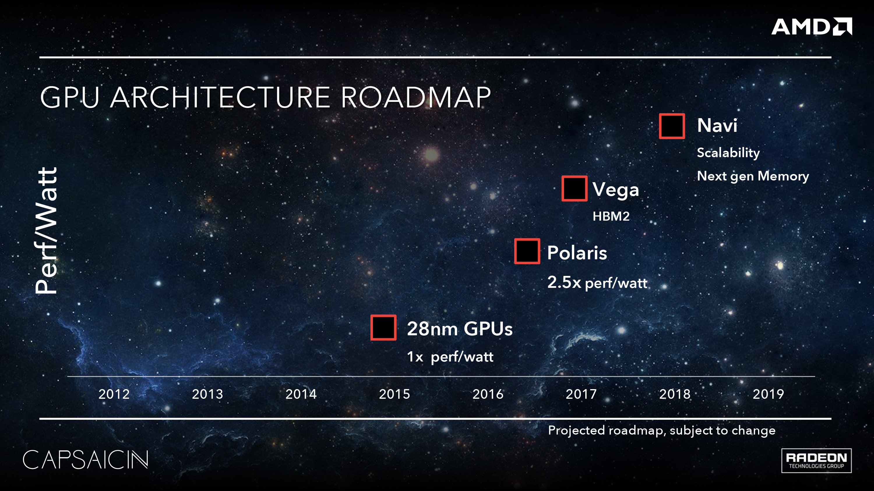
What did that map show us? After 2016’s Polaris would come Vega, and after that would be Navi. As a high-level roadmap it didn’t show us much – in fact other than a timeframe, the only detail attached to Vega was “HBM2” - but it was enough to help understand one of the things AMD would be doing architecturally to set Vega apart from Polaris. As for the timeframe itself, that was ambiguous at best in AMD’s roadmap. But now as we draw closer to the launch of Vega, the picture has become clearer. AMD will be hitting a yearly cadence with Vega. The first chip, which tapped out last year, will be launching in the first half of this year (H1’17).
To that end, with Vega’s launch not too far over the horizon, AMD is ready to start talking about what will be their next GPU architecture. Last year at this time we got our first real glimpse into Polaris and what would become the Radeon RX 480/470/460, and this year AMD is back again with a teaser of things to come with Vega.
Setting The Stage: Expectations Management; Less How & More Why
Before we dive into any architectural details, perhaps it’s best we first set the stage. This goes for both what to expect of today’s announcement, and to better understand what AMD is doing and why.
First and foremost, today’s detail release is a teaser, not a deep dive, or even a preview. AMD is only releasing a few details about Vega, and those are being kept at a high level. In fact it’s fair to say that there’s just enough information to answer little and raise even more questions; just what a proper teaser should be.
Why? Well part of the reason is that we’re still months off from the launch of Vega. I believe it’s fair to say that by announcing a first-half of the year launch date when we’re already in 2017 is a strong indicator that Vega will not launch until later in that window, likely some time in Q2. So we’re still a good three to five months out from the launch of Vega, which means AMD doesn’t want to (or need to) release too many details this far out. Rather they can trickle out chosen details for maximum impact.
At the same time the AMD of 2017 has more they can focus on in the high-performance space than just GPUs. Ryzen launches soon, and they also have other products on the horizon such as the Radeon Instinct accelerators. Polaris received as much detail as it did because it was all AMD really had to talk about, and they needed to recover from a rough 2015 where AMD’s at-the-time power efficiency woes were brought into full focus. But now Vega can share the stage with Ryzen and other products, and that lets AMD be more selective about what they say.
All of which is something I would argue is a good thing. At the end of the day Polaris was an optimized version of the GCN 1.2 (aka GCN 3) architecture for GlobalFoundries’ 14nm FinFET process. The resulting GPUs were solid competitors in the mainstream and value markets, improving on AMD’s power efficiency in a way they badly needed. But they weren’t high-end parts; they didn’t excite like those parts did, and for technology enthusiasts they didn’t significantly change the architecture itself (in fact GCN 4 was ISA compatible with GCN 3, something that doesn’t happen a lot in the GPU space). AMD talked big about Polaris – perhaps too big – and I do think it hurt them in some circles once it became clearer that this was AMD catching up. Which is not to say that AMD’s marketing arm won’t talk big about Vega as well, but they need not ride the technology angle so hard. Vega is a launch that can be more natural and more subdued, especially as at this point we know AMD is aiming big with a much-needed new generation of high-end parts.
In any case, as AMD isn’t riding the technology angle quite as hard in this year’s teaser, they are spending a bit more time explaining the market and some of the logic behind Vega’s design. For its teasing debut, Vega is little less discussion of “how,” and a little more conversation of “why”.
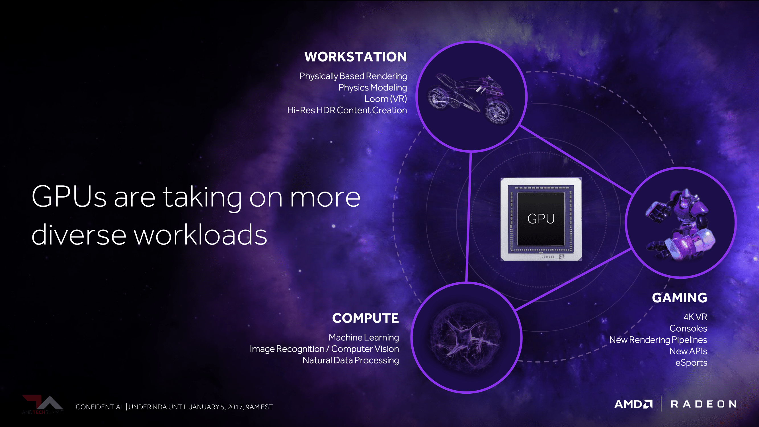
So what is AMD looking to do with Vega? Besides aiming for the high-end of the market, AMD is looking at how the market for GPUs has changed in the last half-decade, and what they need to do to address it. Machine learning is one part of that, being a market that has practically sprung up overnight to become a big source of revenue for GPUs. This is where the previously announced Radeon Instinct will fit in.
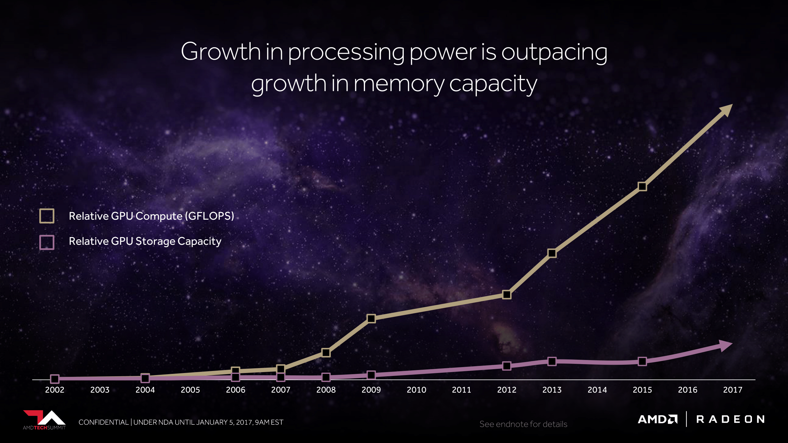
But more than that, it’s about fundamental shifts in how workloads are structured. GPU performance growth has far outpaced GPU memory capacity. Scene geometry complexity has continued to grow. Newer rendering methods have significantly changed GPU memory access patterns.
To that end, AMD is looking to address all of these factors with Vega. Which is not to say that this is everything – this is a teaser, after all – but this is where AMD is starting. Where they are going to be with their next generation architecture and how they believe it will address the changes in the market. So without further ado, let’s take a teasing look at what the future has in store for AMD’s GPUs.
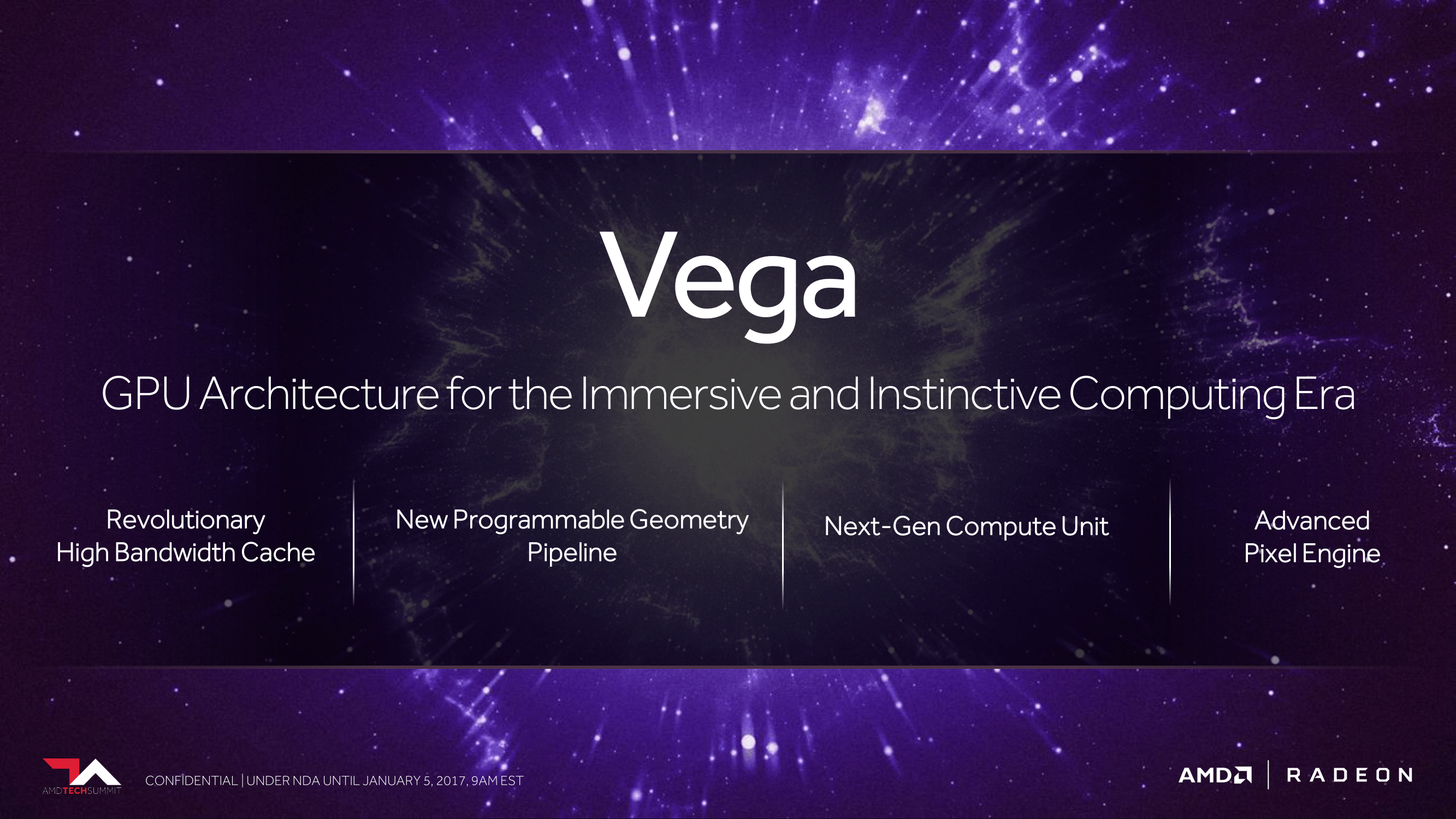
Vega’s NCU: Packed Math, Higher IPC, & Higher Clocks
As always, I want to start at the heart of the matter: the shader core. In some respects AMD has not significantly altered their shader core since the launch of the very first GCN parts 5 years ago. Various iterations of GCN have added new instructions and features, but the shader core has remained largely constant, and IPC within the shader core itself hasn’t changed too much. Even Polaris (GCN 4) followed this trend, sharing its whole ISA with GCN 1.2.
With Vega, this is changing. By just how much remains to be seen, but it is clear that even with what we see today, AMD is already undertaking the biggest change to their shader core since the launch of GCN.
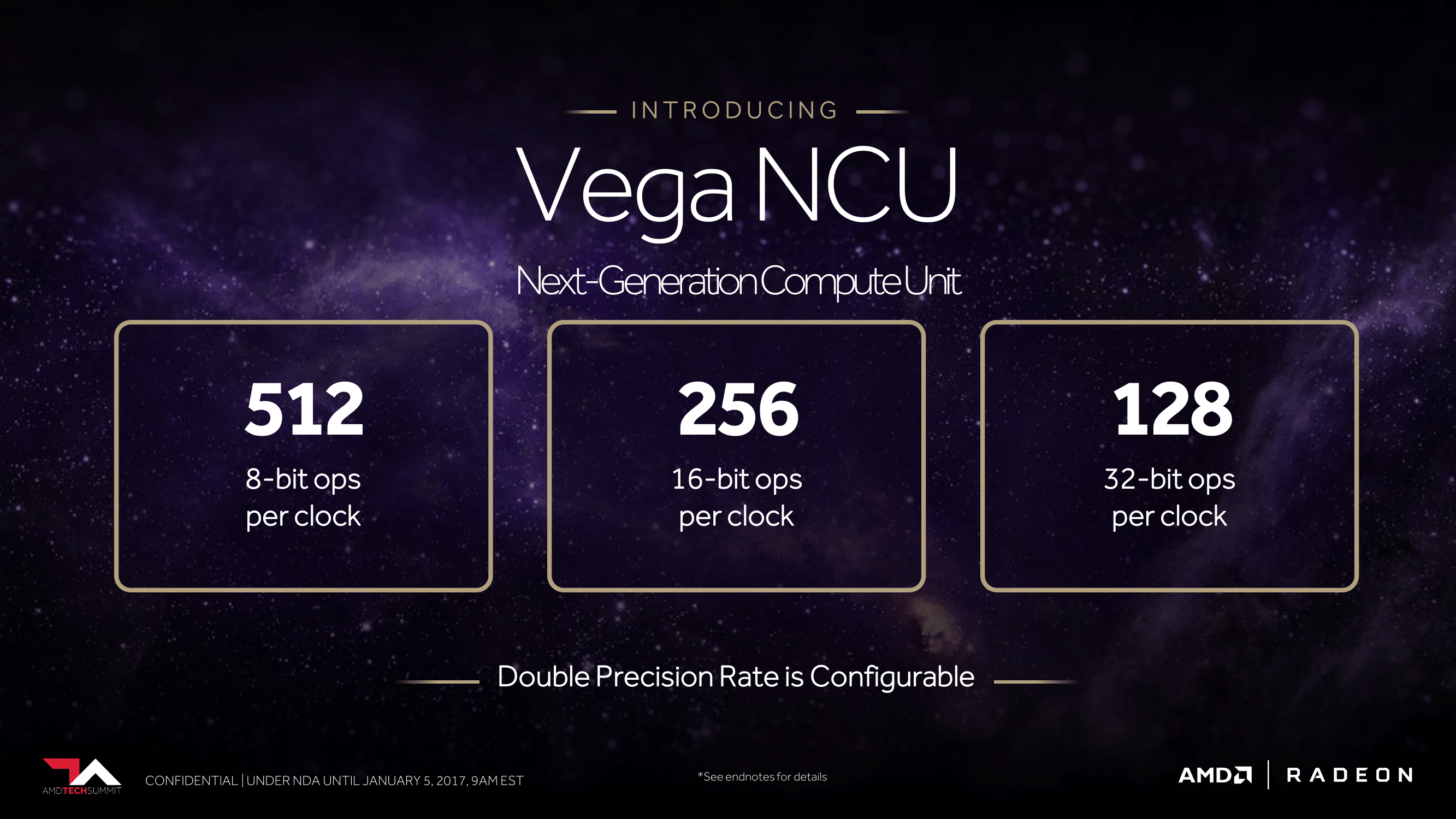
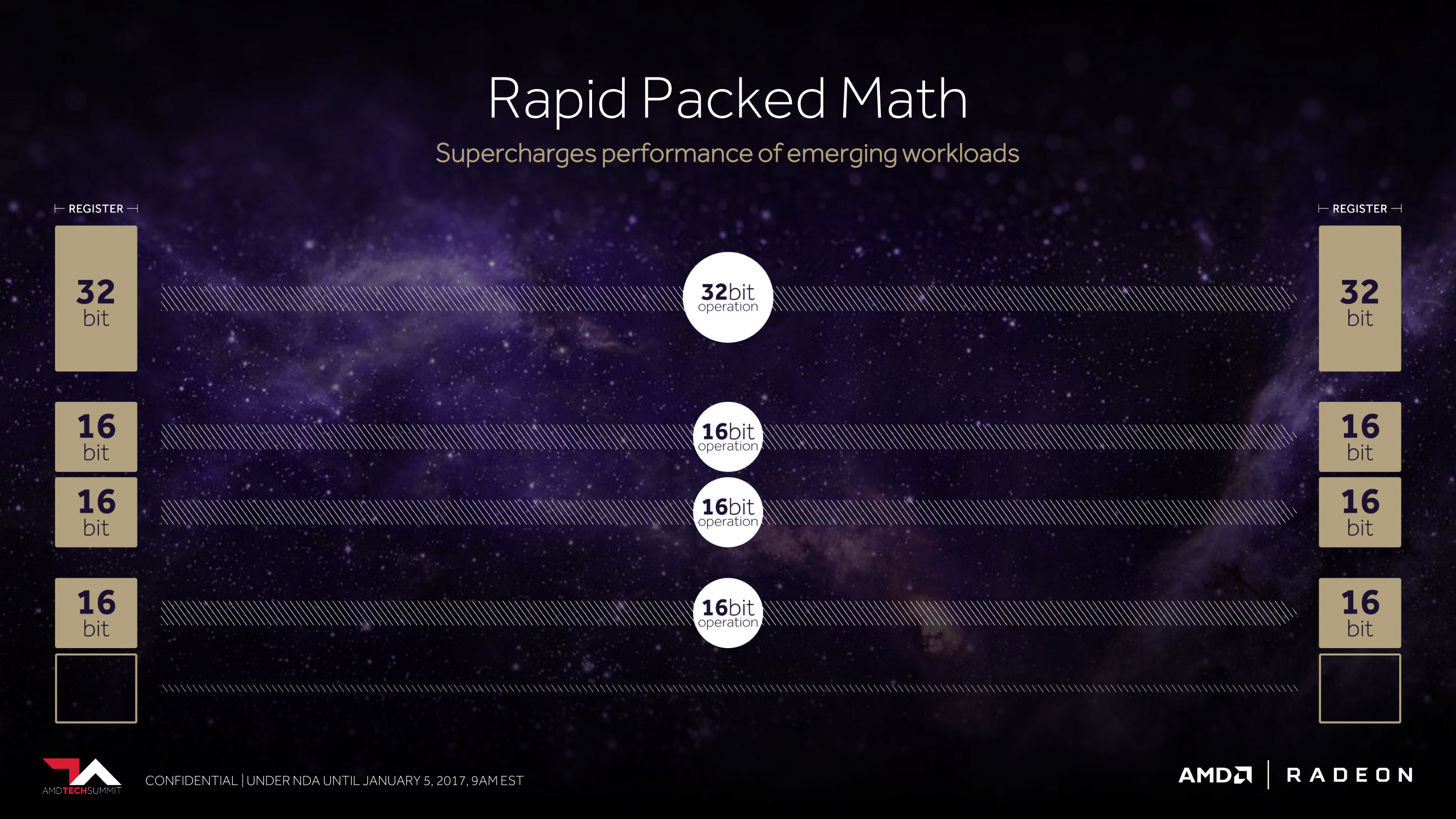
Meet the NCU, Vega’s next-generation compute unit. As we already learned from the PlayStation 4 Pro launch and last month’s Radeon Instinct announcement, AMD has been working on adding support for packed math formats for future architectures, and this is coming to fruition in Vega.
With their latest architecture, AMD is now able to handle a pair of FP16 operations inside a single FP32 ALU. This is similar to what NVIDIA has done with their high-end Pascal GP100 GPU (and Tegra X1 SoC), which allows for potentially massive improvements in FP16 throughput. If a pair of instructions are compatible – and by compatible, vendors usually mean instruction-type identical – then those instructions can be packed together on a single FP32 ALU, increasing the number of lower-precision operations that can be performed in a single clock cycle. This is an extension of AMD’s FP16 support in GCN 1.2 & GCN 4, where the company supported FP16 data types for the memory/register space savings, but FP16 operations themselves were processed no faster than FP32 operations.
And while previous announcements may have spoiled that AMD offers support for packed FP16 formats, what we haven’t known for today is that they will also support a high-speed path (analogous to packed FP16) for 8-bit integer operations. INT8 is a data format that has proven especially useful for neural network inference – the actual execution of trained neural networks – and is a major part of what has made NVIDIA’s most recent generation of Pascal GPUs so potent at inferencing. By running dot products and certain other INT8 operations along this path, INT8 performance can be greatly improved.
Though before we get too far – and this is a longer discussion to have closer to Vega’s launch – it’s always important to note when and where these faster operations can be used in consumer workloads, as the odds are most of you reading this are thinking gaming. While FP16 operations can be used for games (and in fact are in the mobile space), in the PC space they are virtually never used. When PC GPUs made the jump to unified shaders in 2006/2007, the decision was made to do everything at FP32 since that’s what vertex shaders typically required to begin with, and it’s only recently that anyone has bothered to look back. So while there is some long-term potential here for Vega’s fast FP16 math to become relevant for gaming, at the moment it wouldn’t do anything. Vega will almost certainly live and die in the gaming space based on its FP32 performance.
Moving on, the second thing we can infer from AMD’s slide is that a CU on Vega is still composed of 64 ALUs, as 128 FP32 ops/clock is the same rate as a classic GCN CU. Nothing here is said about how the Vega NCU is organized – if it’s still four 16-wide vector SIMDs – but we can at least reason out that the total size hasn’t changed.
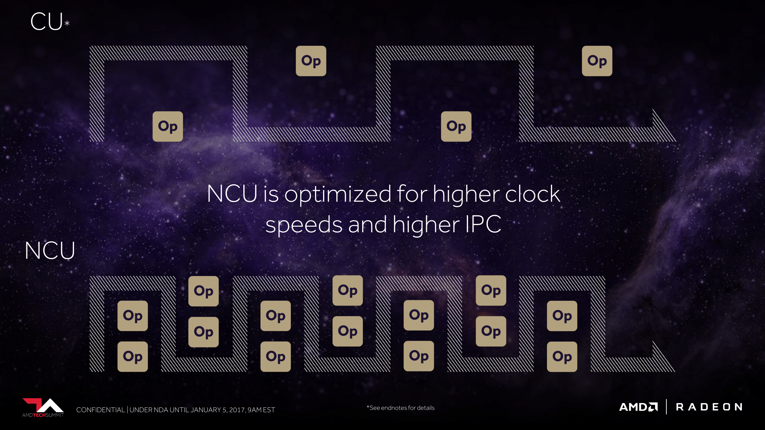
Finally, along with outlining their new packed math formats, AMD is also confirming, at a high level, that the Vega NCU is optimized for both higher clockspeeds and a higher IPC. It goes without saying that both of these are very important to overall GPU performance, and it’s an area where, very broadly speaking, AMD hasn’t compared to NVIDIA too favorably. The devil is in the details, of course, but a higher clockspeed alone would go a long way towards improving AMD’s performance. And as AMD’s IPC has been relatively stagnant for some time here, improving it would help AMD put their relatively sizable lead in total ALUs to good use. AMD has always had a good deal more ALUs than a comparable NVIDIA chip, but getting those ALUs to all do useful work outside of corner cases has always been difficult.
That said, I do think it’s important not to read too much into this on the last point, especially as AMD has drawn this slide. It’s fairly muddled whether “higher IPC” means a general increase in IPC, or if AMD is counting their packed math formats as the aforementioned IPC gain.
Geometry & Load Balancing: Faster Performance, Better Options
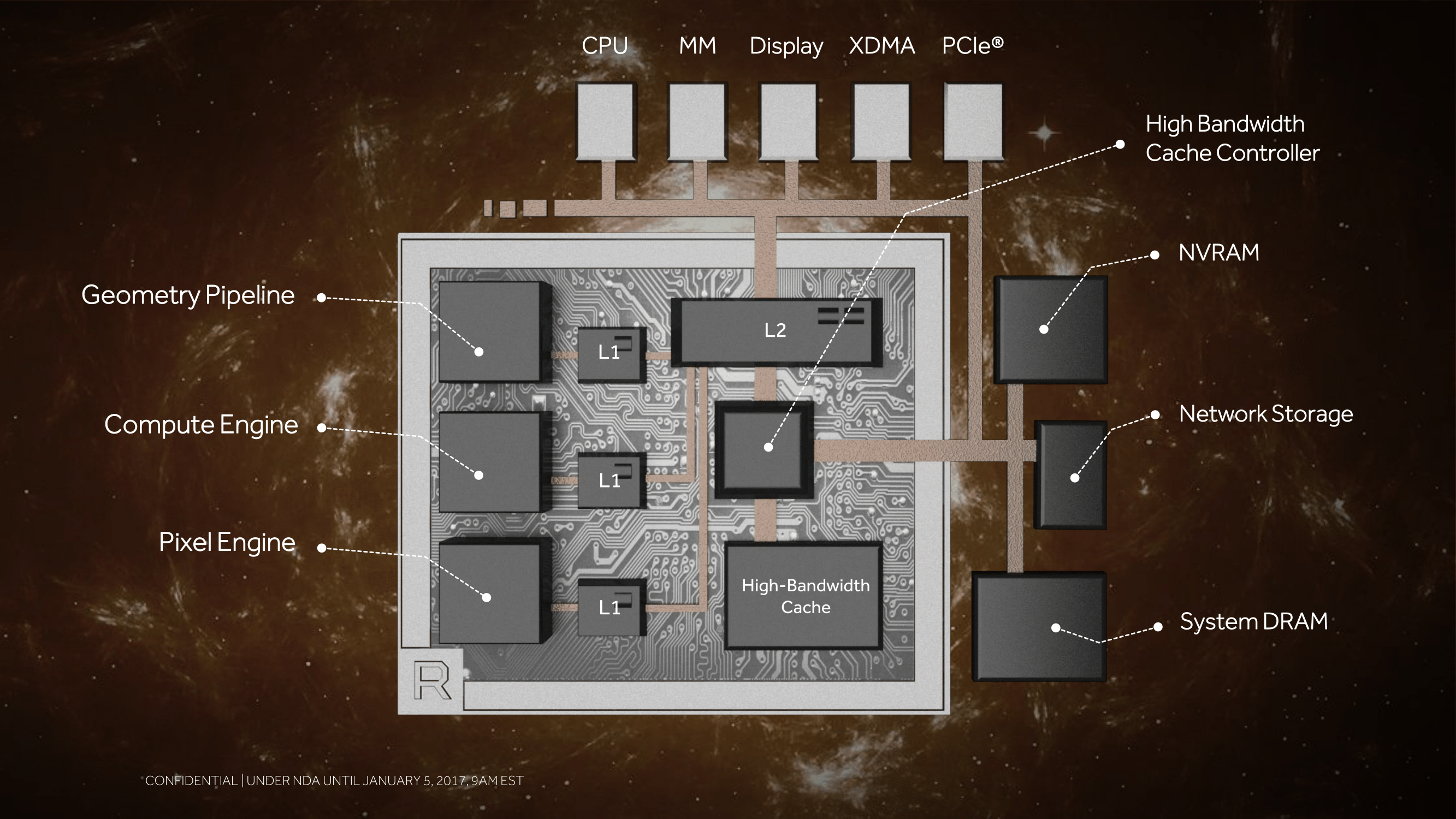
As some of our more astute readers may recall, when AMD launched the GCN 1.1 they mentioned that at the time, GCN could only scale out to 4 of what AMD called their Shader Engines; the logical workflow partitions within the GPU that bundled together a geometry engine, a rasterizer, CUs, and a set of ROPs. And when the GCN 1.2 Fiji GPU was launched, while AMD didn’t bring up this point again, they still held to a 4 shader engine design, presumably due to the fact that GCN 1.2 did not remove this limitation.
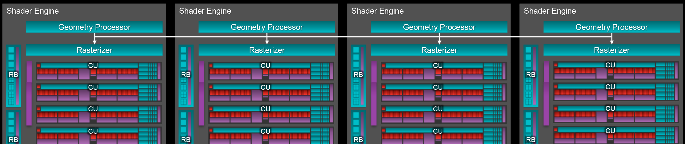
Fiji 4x Shader Engine Layout
But with Vega however, it looks like that limitation has finally gone away. AMD is teasing that Vega offers an improved load balancing mechanism, which pretty much directly hints that AMD can now efficiently distribute work over more than 4 engines. If so, this would represent a significant change in how the GCN architecture works under the hood, as work distribution is very much all about the “plumbing” of a GPU. Of the few details we do have here, AMD has told us that they are now capable of looking across draw calls and instances, to better split up work between the engines.
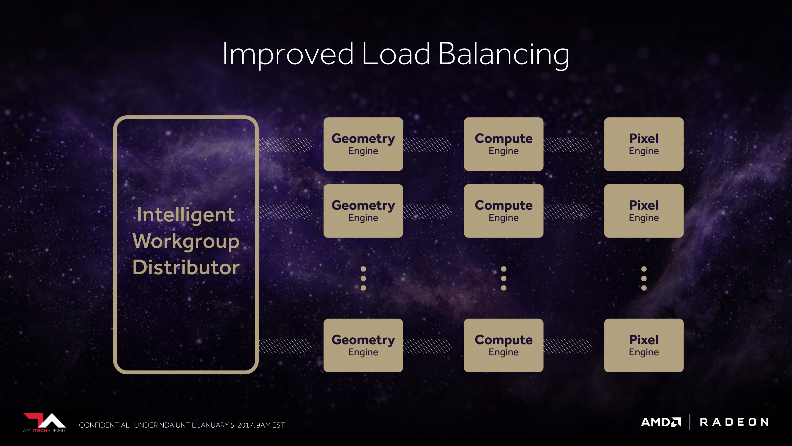
This in turn is a piece of the bigger picture when looking at the next improvement in Vega, which is AMD’s geometry pipeline. Overall AMD is promising a better than 2x improvement in peak geometry throughput per clock. Broadly speaking, AMD’s geometry performance in recent generations hasn’t been poor (it’s one of the areas where Polaris even further improved), but it has also hurt them at times. So this is potentially important for removing a bottleneck to squeezing more out of GCN.
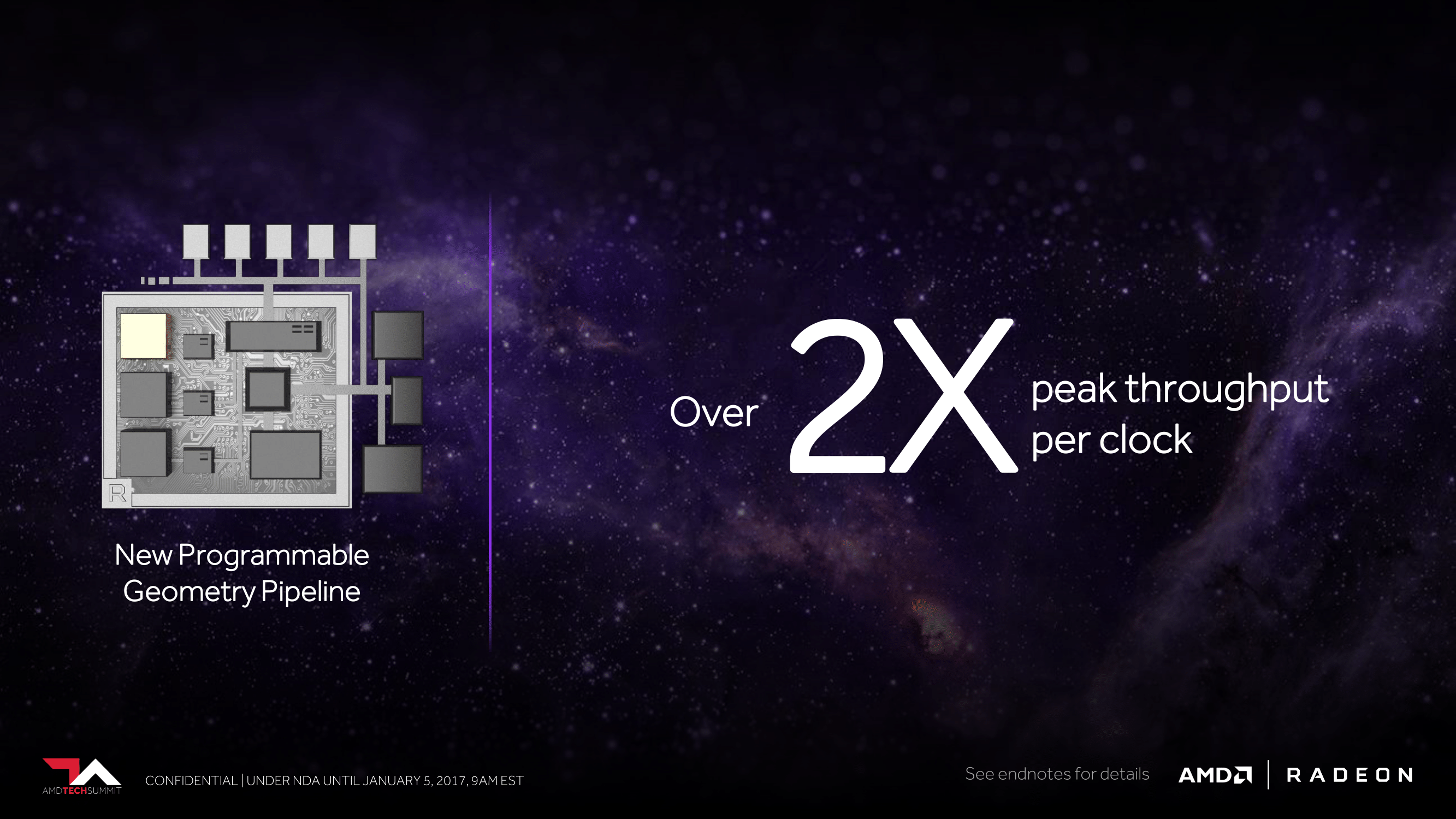
And while AMD's presentation and comments itself don't go into detail on how they achieved this increase in throughput, buried in the footnote for AMD's slide deck is this nugget: "Vega is designed to handle up to 11 polygons per clock with 4 geometry engines." So this clearly reinforces the idea that the overall geometry performance improvement in Vega comes from improving the throughput of the individual geometry engines, as opposed to simply adding more as the scalability improvements presumably allow. This is one area where Vega’s teaser paints a tantalizing view of future performance, but in the process raises further questions on just how AMD is doing it.
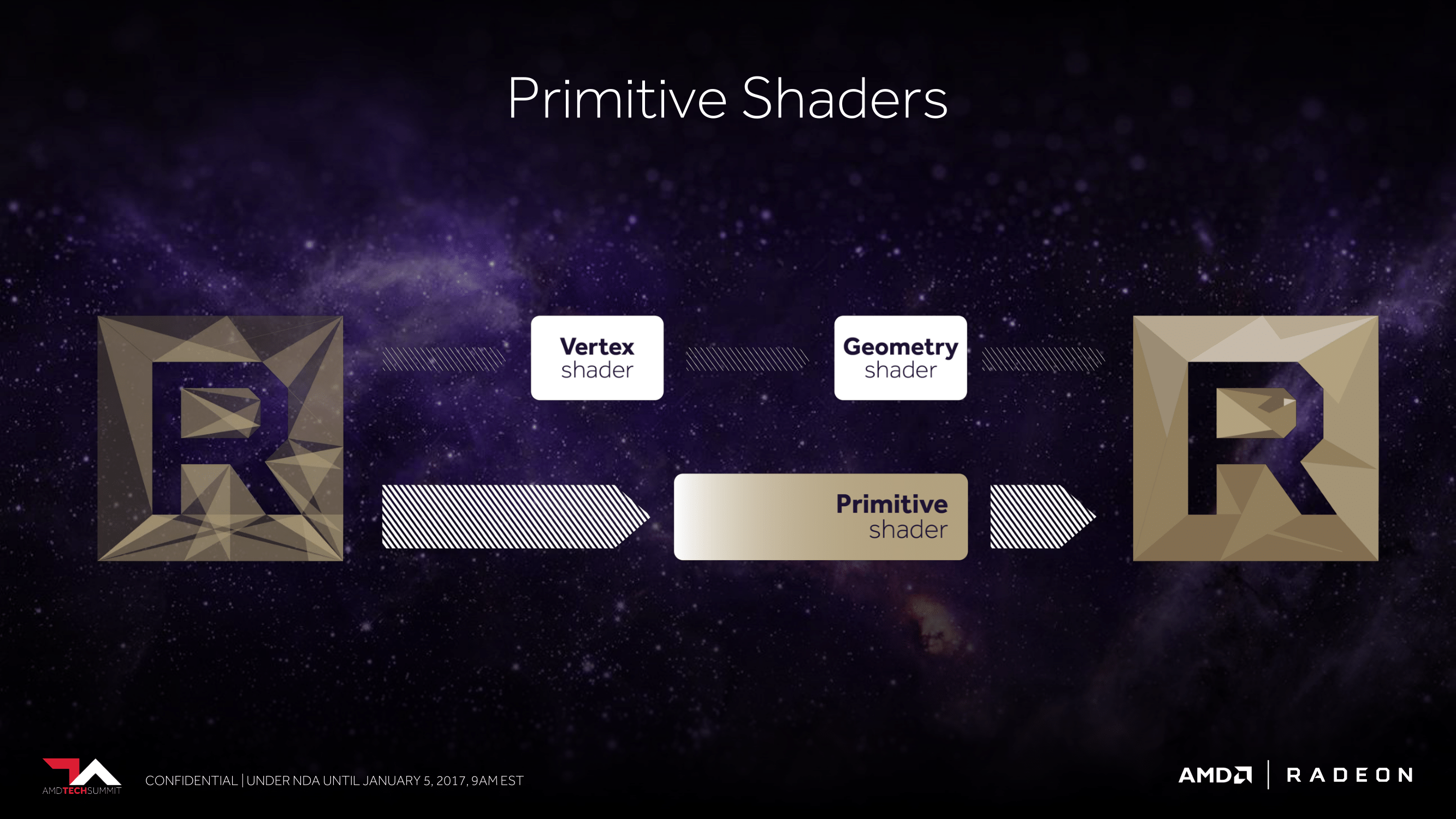
In any case, however AMD is doing it, the updated geometry engines will also feature one more advancement, which AMD is calling the primitive shader. A new shader stage that runs in place of the usual vertex and geometry shader path, the primitive shader allows for the high speed discarding of hidden/unnecessary primitives. Along with improving the total primitive rate, discarding primitives is the next best way to improve overall geometry performance, especially as game geometry gets increasingly fine, and very small, overdrawn triangles risk choking the GPU.
AMD isn’t offering any real detail here in how the primitive shader operates, and as a result I’m curious here whether this is something that AMD’s shader compiler can automatically add, or if it requires developers to specifically call it (like they would vertex and geometry shaders).
HBM2 & “The World’s Most Scalable GPU Memory Architecture”
With the launch of the Fiji GPU and resulting Radeon R9 Fury products in 2015, AMD became the first GPU manufacturer to ship with first-generation High Bandwidth Memory (HBM). The ultra-wide memory standard essentially turned the usual rules of GPU memory on its head, replacing narrow, high clocked memory (GDDR5) with wide, low clocked memory. By taking advantage of Through Silicon Vias (TSVs) and silicon interposers, HBM could offer far more bandwidth than GDDR5 while consuming less power and taking up less space.
Now for Vega, AMD is back again with support for the next generation of HBM technology, HBM2. In fact this is the very first thing we ever learned about Vega, going back to AMD’s roadmap from last year where it was the sole detail listed for the architecture.
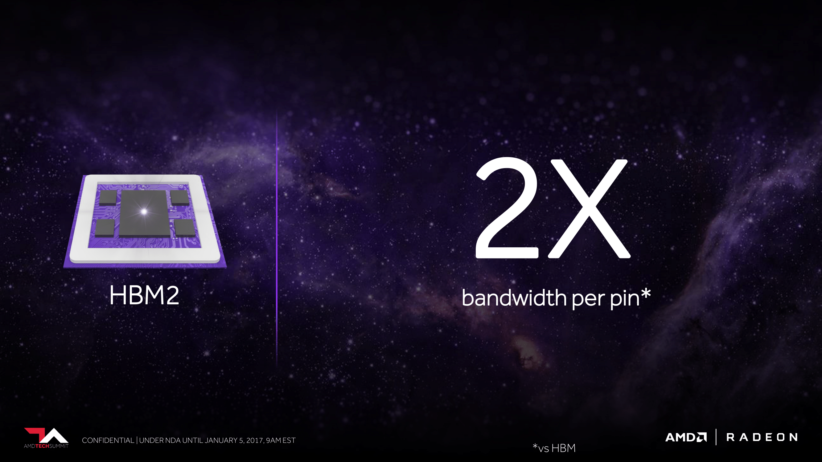
HBM2 builds off of HBM, offering welcome improvements in both bandwidth and capacity. In terms of bandwidth, HBM2 can clock at up to 2Gbps per pin, twice the rate of HBM1. This means that at those clockspeeds (and I’ll note that at least so far we haven’t seen any 2Gbps HBM2), AMD can either double their memory bandwidth or cut the number of HBM stacks they need in half to get the same amount of bandwidth. The latter point is of particular interest, as we’ll get to here in a bit.
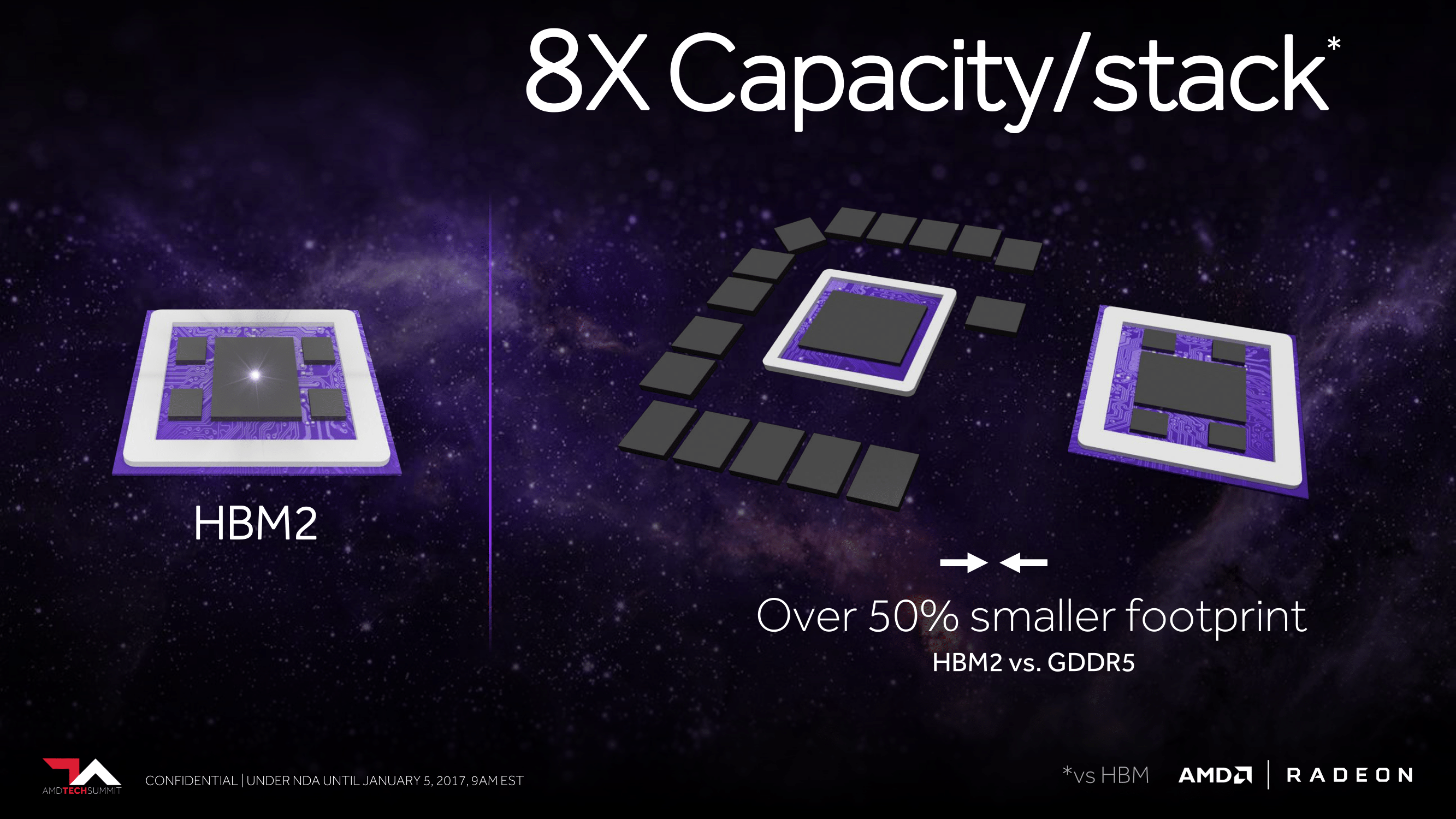
But more important still are the capacity increases. HBM1 stacked topped out at 1GB each, which means Fiji could have no more than 4GB of VRAM. HBM2 stacks go much higher – up to 8GB per stack – which means AMD’s memory capacity problems when using HBM have for all practical purposes gone away. AMD could in time offer 8GB, 16GB, or even 32GB of HBM2 memory, which is more than competitive with current GDDR5 memory types.
Meanwhile it’s very interesting to note that with Vega, AMD is calling their on-package HBM stacks “high-bandwidth cache” rather than “VRAM” or similar terms as was the case with Fiji products.
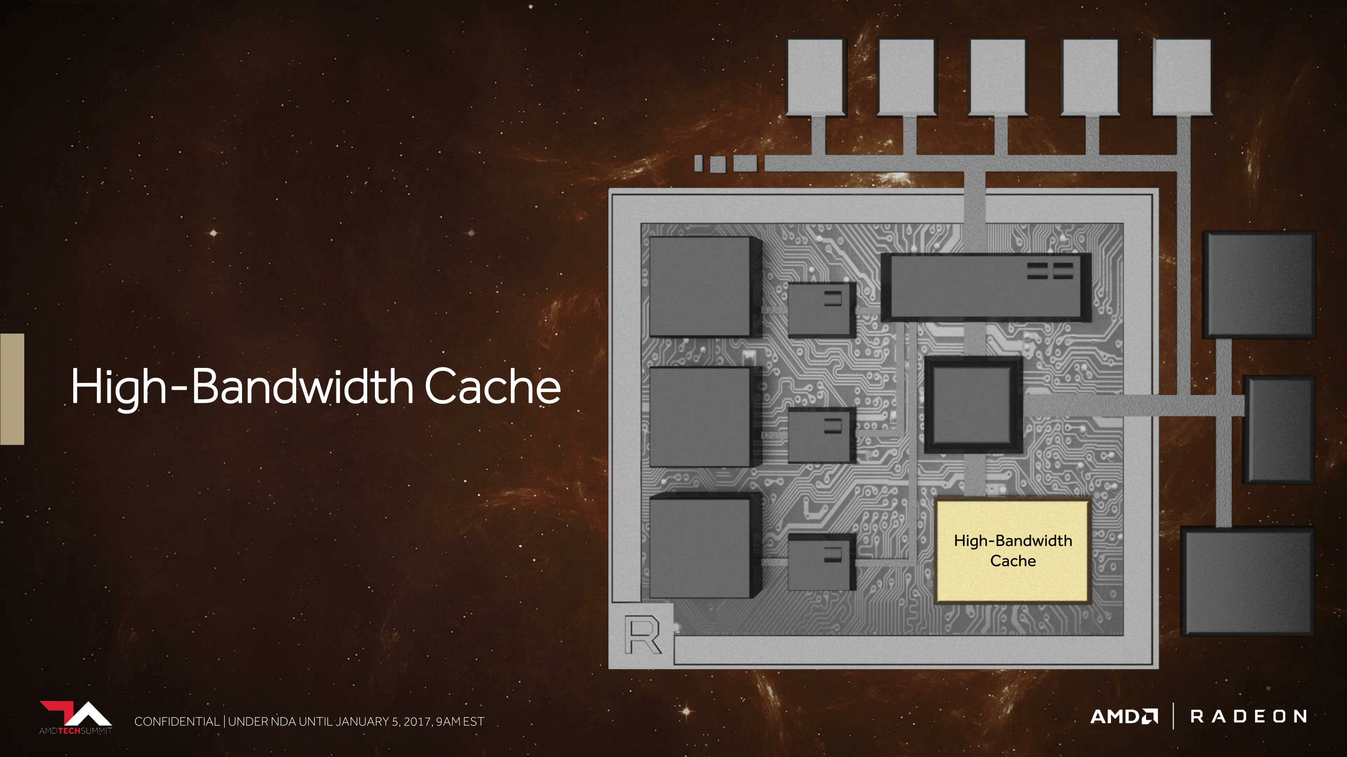
This is a term that can easily be misread – and it’s the one area where perhaps it’s too much of a tease – but despite the name, there are no signals from AMD right now that it’s going to be used as a cache in the pure, traditional sense. Rather, because AMD has already announced that they’re looking into other ideas such as on-card NAND storage (the Radeon Pro SSG), they are looking at memory more broadly.
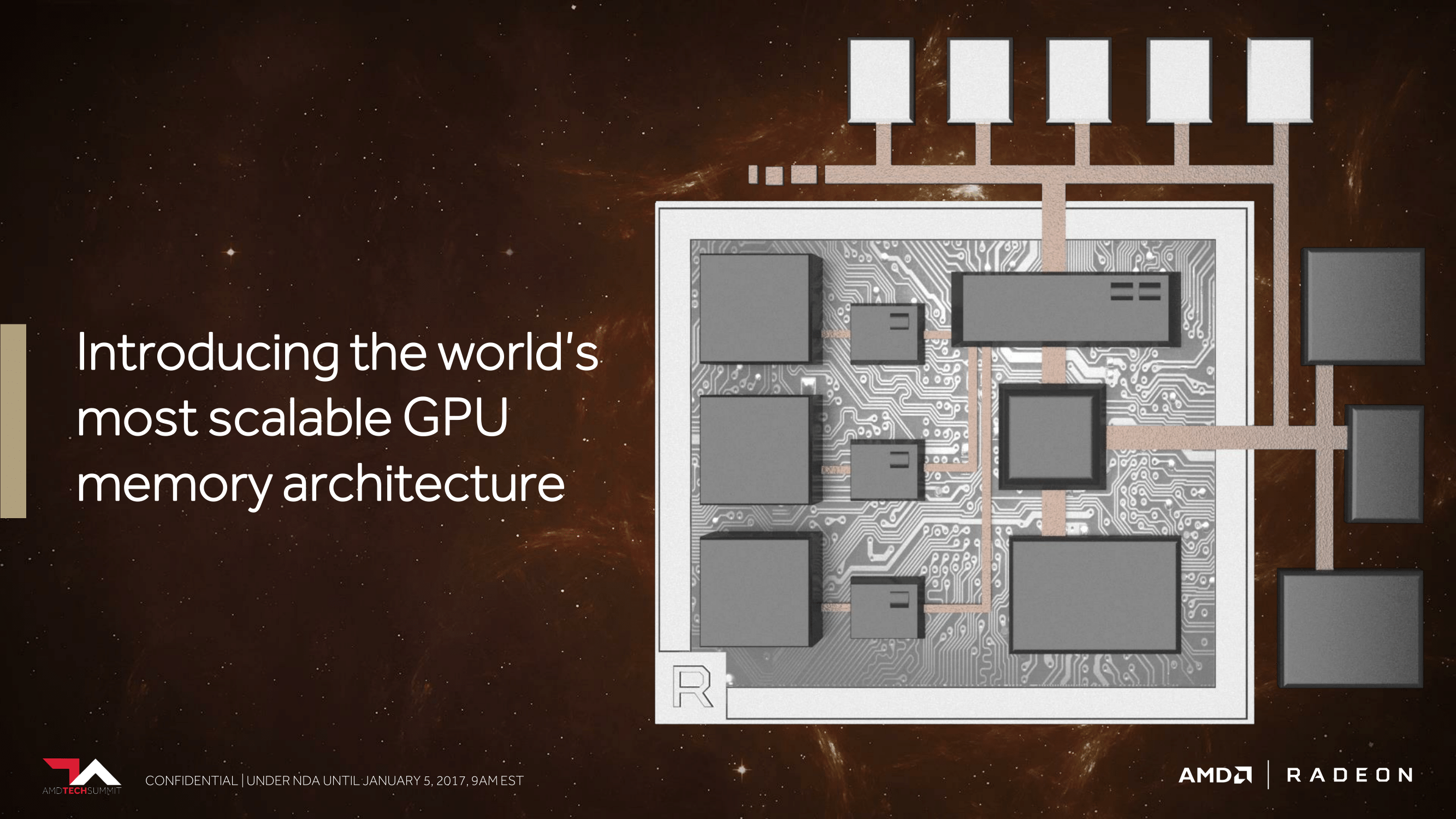
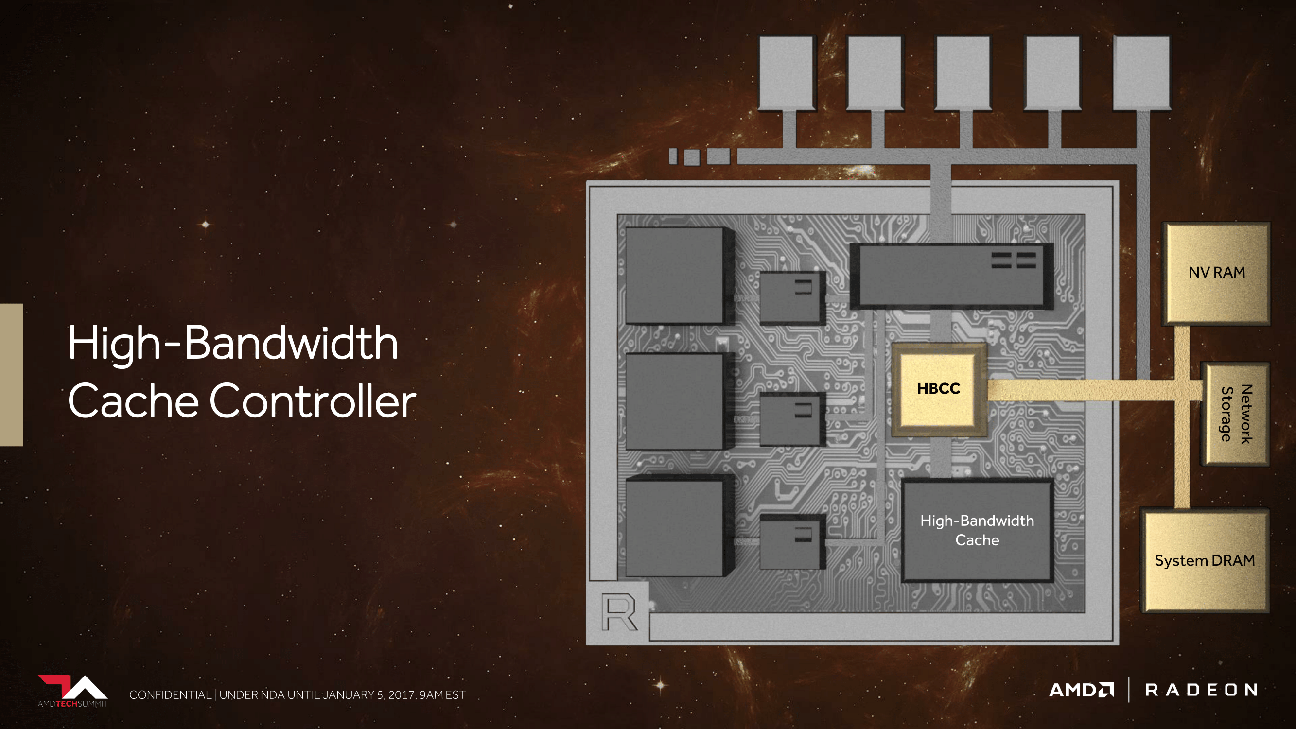
And this brings us to what AMD is calling “The World’s Most Scalable GPU Memory Architecture”. Along with supporting HBM, AMD has undertaken a lot of under-the-hood work to better support large dataset management between the high bandwidth cache (HBM2), on-card NAND, and even farther out sources like system RAM and network storage.
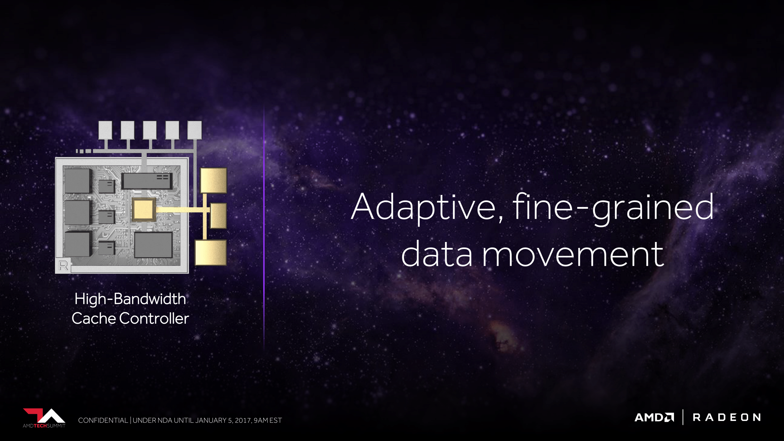
The basic idea here is that, especially in the professional space, data set size is vastly larger than local storage. So there needs to be a sensible system in place to move that data across various tiers of storage. This may sound like a simple concept, but in fact GPUs do a pretty bad job altogether of handling situations in which a memory request has to go off-package. AMD wants to do a better job here, both in deciding what data needs to actually be on-package, but also in breaking up those requests so that “data management” isn’t just moving around a few very large chunks of data. The latter makes for an especially interesting point, as it could potentially lead to a far more CPU-like process for managing memory, with a focus on pages instead of datasets.
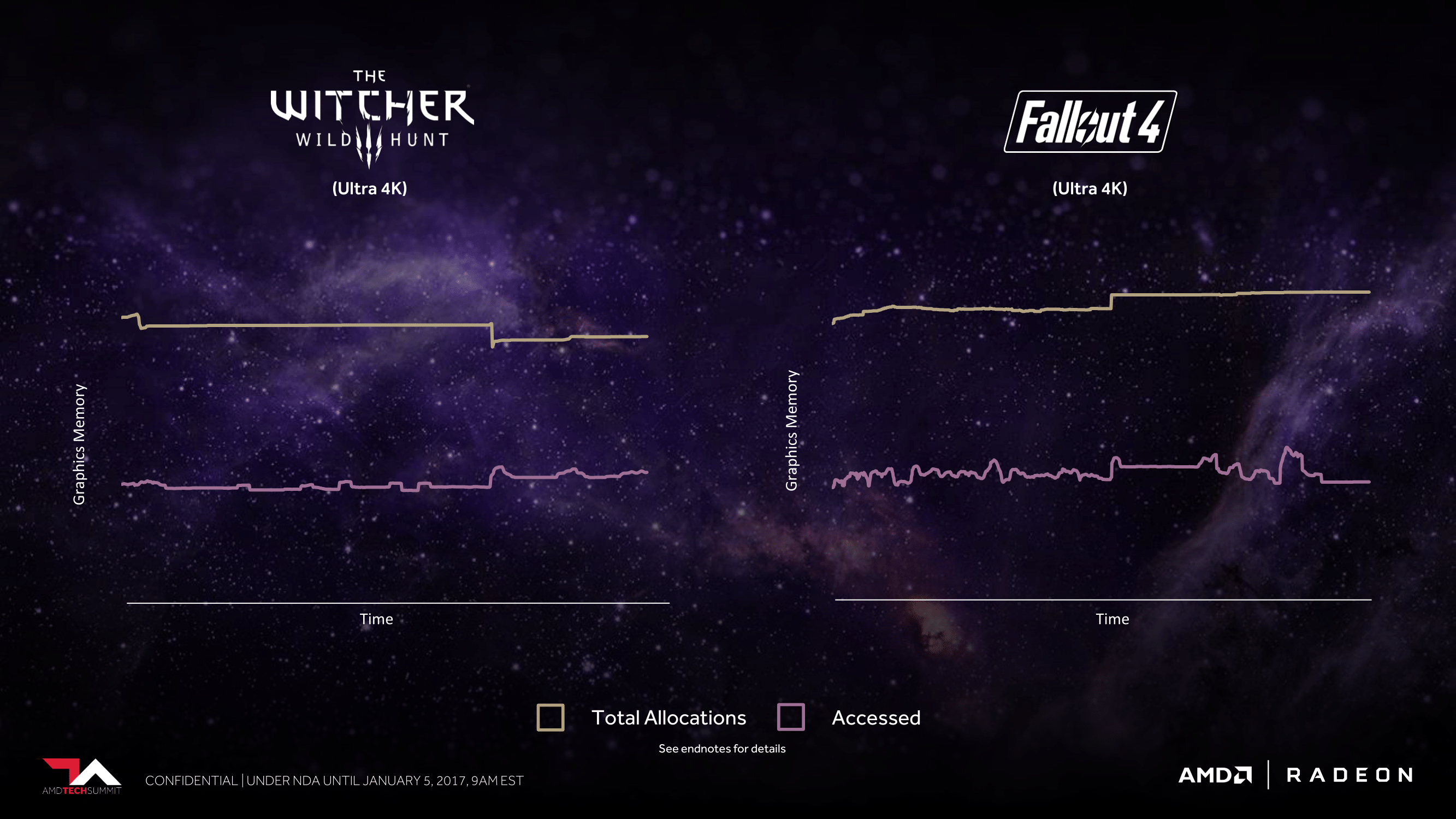
Interestingly, to drive this point home, AMD actually turned to games rather than professional applications. Plotting out the memory allocation and usage patterns of The Witcher III and Fallout 4, AMD finds that both games allocate far more memory than they actually use, by nearly a factor of 2x. Part of this is undoubtedly due to the memory management model of the DirectX 11 API used by both games, but a large factor is also simply due to the fact that this is traditionally what games have always done. Memory stalls are expensive and games tend to be monolithic use cases, so why not allocate everything you can, just to be sure you don’t run out?
The end result here is that AMD is painting a very different picture for how they want to handle memory allocations and caching on Vega and beyond. In the short term it’s professional workloads that stand to gain the most, but in the long run this is something that could impact games as well. And not to be ignored is virtualization; AMD’s foray into GPU virtualization is still into its early days, but this likely will have a big impact on virtualization as well. In fact I imagine it’s a big reason why AMD is giving Vega the ability to support a relatively absurd 512TB of virtual address space, many times the size of local VRAM. Multi-user time-sharing workloads are a prime example of where large address spaces can be useful.
ROPs & Rasterizers: Binning for the Win(ning)
We’ll suitably round-out our overview of AMD’s Vega teaser with a look at the front and back-ends of the GPU architecture. While AMD has clearly put quite a bit of effort into the shader core, shader engines, and memory, they have not ignored the rasterizers at the front-end or the ROPs at the back-end. In fact this could be one of the most important changes to the architecture from an efficiency standpoint.
Back in August, our pal David Kanter discovered one of the important ingredients of the secret sauce that is NVIDIA’s efficiency optimizations. As it turns out, NVIDIA has been doing tile based rasterization and binning since Maxwell, and that this was likely one of the big reasons Maxwell’s efficiency increased by so much. Though NVIDIA still refuses to comment on the matter, from what we can ascertain, breaking up a scene into tiles has allowed NVIDIA to keep a lot more traffic on-chip, which saves memory bandwidth, but also cuts down on very expensive accesses to VRAM.
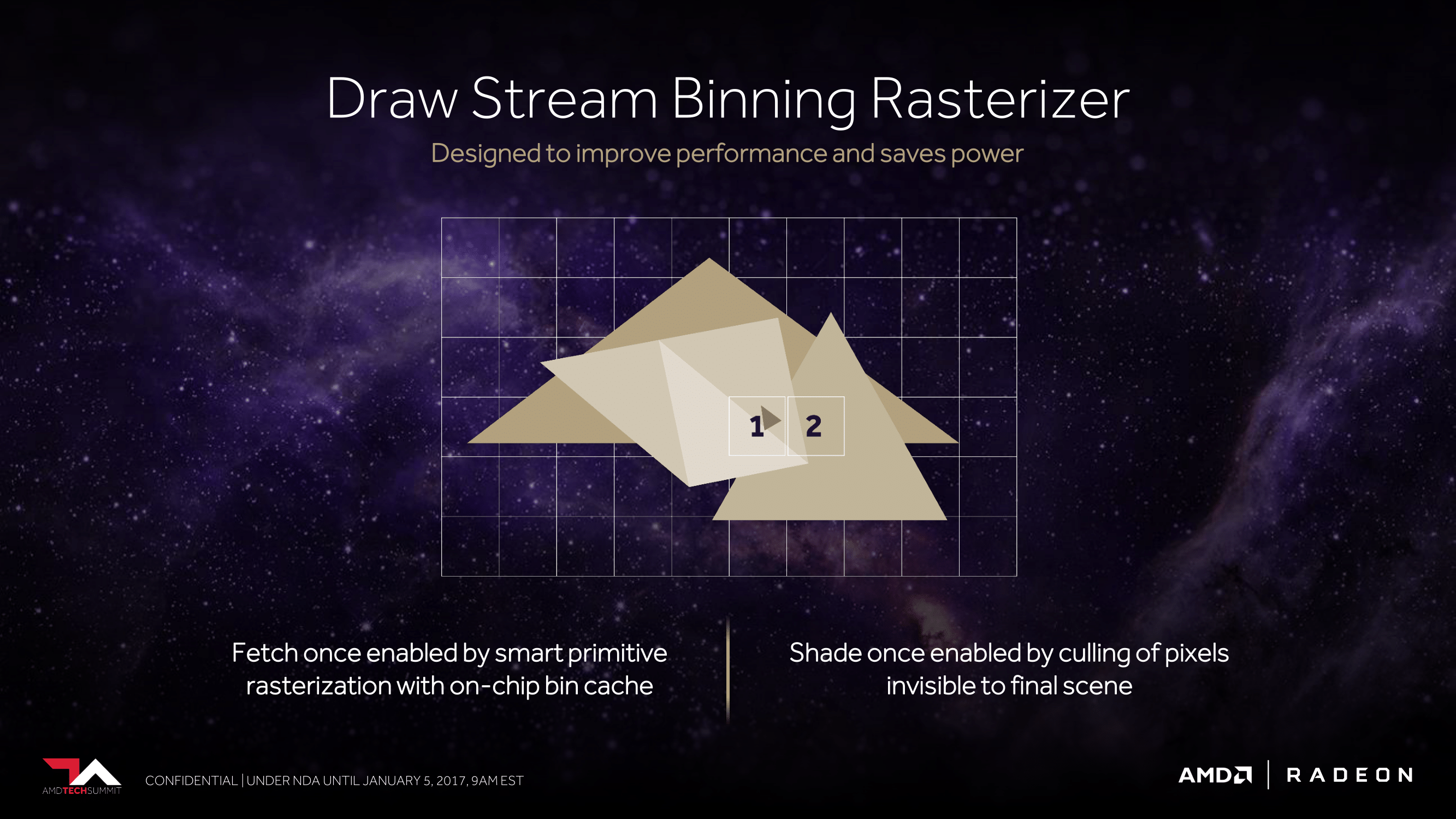
For Vega, AMD will be doing something similar. The architecture will add support for what AMD calls the Draw Stream Binning Rasterizer, which true to its name, will give Vega the ability to bin polygons by tile. By doing so, AMD will cut down on the amount of memory accesses by working with smaller tiles that can stay-on chip. This will also allow AMD to do a better job of culling hidden pixels, keeping them from making it to the pixel shaders and consuming resources there.
As we have almost no detail on how AMD or NVIDIA are doing tiling and binning, it’s impossible to say with any degree of certainty just how close their implementations are, so I’ll refrain from any speculation on which might be better. But I’m not going to be too surprised if in the future we find out both implementations are quite similar. The important thing to take away from this right now is that AMD is following a very similar path to where we think NVIDIA captured some of their greatest efficiency gains on Maxwell, and that in turn bodes well for Vega.
Meanwhile, on the ROP side of matters, besides baking in the necessary support for the aforementioned binning technology, AMD is also making one other change to cut down on the amount of data that has to go off-chip to VRAM. AMD has significantly reworked how the ROPs (or as they like to call them, the Render Back-Ends) interact with their L2 cache. Starting with Vega, the ROPs are now clients of the L2 cache rather than the memory controller, allowing them to better and more directly use the relatively spacious L2 cache.

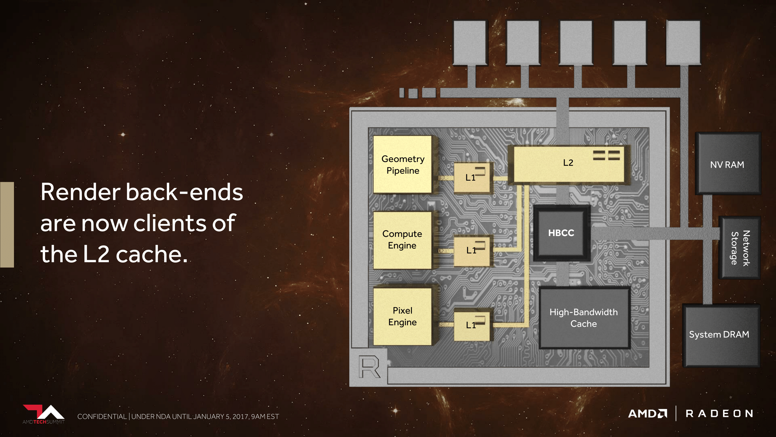
This is especially significant for a specific graphics task, which is rendering to a texture (as opposed to a frame buffer to be immediately displayed). Render to texture is an especially common operation for deferred shading, and while deferred shading itself isn’t new, its usage is increasing. With this change to Vega, the ROPs can now send a scene rendered to a texture to the L2 cache, which can in turn be fetched by the texture units for reuse in the next stage of the rendering process. Any potential performance improvements from this change are going to be especially game-specific since not every game uses deferred shading, but it’s one of those corner cases that is important for AMD to address in order to ensure more consistent performance.
First Thoughts: A Peek At What’s To Come
Wrapping things up, while today’s reveal from AMD is only a teaser of what they have been working on over the last few years with Vega, it’s none the less an important one. Based on what we know so far, Vega stands to be the biggest change to AMD’s GPU architecture since GCN 1.0 was released 5 years ago, and the changes to the ALUs, the ROPs, the memory structure, and other aspects of Vega reinforce this notion. To be sure, Vega is not a wholly new architecture – it is clearly a further refinement of GCN – but then this is exactly why GCN was designed to be able to evolve through refinements over a very long period of time.
What we have for now then is a quick look at what’s to come from AMD. There are still many things we don’t know, not the least of which is the actual GPU configurations. But for a teaser it’s enough to show that AMD has been hard at work. It sets the stage for the hardware and marketing ramp-up to come over the next few months.
But for now, let’s close with an image. As I mentioned before, the first Vega has taped out, and Radeon Technology Group’s frontman and Chief Architect, Raja Koduri, has one. The chip was just a few weeks old as of December, and while trying to discern die size may be a little too error-prone, we can see one important detail: 2 HBM2 packages.

Raja and AMD will not tell us what chip we’re looking at – like Polaris, two Vega chips have been confirmed – but either way we are looking at one of them in all its alpha silicon glory. Bearing in mind HBM2’s much greater bandwidth per pin, we could very well be looking at a design for a Fiji-like 512GB/sec of memory bandwidth in the chip Raja holds. And for AMD, that is one more teaser for today to keep attention focused right where they want it: on Vega ahead of its H1’17 launch.


